Reverse engineering embedded software
Embedded devices usually contain the same elements that make up larger, more general purpose systems, such as a processor, ROM, RAM, network controllers etc. Sometimes these are contained within a custom-designed integrated circuit, such as an ASIC. In these situations, it is very hard to get access to information about what is running inside. But in other cases, some or all of the components are provided in standard, off-the-shelf components which can make access much easier. In these circumstances, it can be possible to extract the software from the system and learn about how it was constructed and how it operates.
There are some notable instances of devices that have been reverse engineered to such an extent that people have replaced or augmented the software. A couple of notable examples are Canon digital cameras which can run enhanced software (Magic Lantern and CHDK) and Linksys routers with custom firmware installed (OpenWRT). Of course, it takes a lot of effort, skill and perseverance to get to that point, but as is often the case with these kinds of things, it is the journey that can be most interesting.
Before you start…
Before you start, you need to remember that reverse engineering a device is probably not what the manufacturer would prefer that you do. In some places, it may not even be legal to open up that hardware and to extract the contents. So, you need to think about the legal aspects of what you are doing. Now, even if it is lawful to reverse engineer an embedded device, disseminating the software contained within is almost certainly going to violate copyright laws. Personally, I’m happy to respect the rights of the manufacturer and to not make their software public. That’s not to say that I can’t write about what I’ve found out.
So that’s the important stuff out of the way.
My approach
One of my hobbies is prototyping electronic stuff, so I’m reasonably comfortable playing about with things like microcontrollers, breadboards, datasheets etc, and am pretty good at holding the right end of a soldering iron. So, my preferred approach to attacking a system is to dive in, extract the chip containing the software and suck out the contents directly. Here’s how I go about it.
Identify the target
Before you start, you want to do some reconnaissance. Get access to the main PCB, preferably by removing it from the device (so you can see both sides). If you do remove the board, do try to use some static protection, for example, a grounded wrist-strap at the least. I also work on an antistatic mat on my workbench. It would be a shame to find that you couldn’t get anything out because your nylon shirt and running shoes conspired to zap the chip you’re interested in into oblivion… Also, you might want to put it together again, so make a note of all the connectors that you removed.
Have a good look at the board. You want to identify as many chips as you can. Get their ID codes and Google them to see if you can find out what they do, and – ideally – download a datasheet. The smaller the chip, the more likely that the ID will be abbreviated, so finding information can be a bit of a black art. Get familiar with chip vendor logos, so that you can work out who made it; that can help you find the right datasheet. Often there’ll be some big square chip with lots of pins (or lots of solder balls underneath), that you can’t identify. That is often the custom ASIC, and only the manufacturer will know anything about it, and they won’t tell you 🙂 To get the software, your best target is a ROM or Flash RAM chip. These tend to have easily accessible datasheets. There may also be one or more DRAM chips. Their ID codes and datasheets will be relatively easy to find, but they aren’t much use to you in this situation.
Extract the ROM / Flash RAM chip
If you have identified a ROM or Flash RAM chip, you’ve likely found a good place for some software. If you have a Flash RAM chip, the device is likely to be upgradable via a firmware update. Once I’ve also got the datasheet for the device, the next step is to de-solder it from the board. You can use a hot air de-solderer, or just use a soldering iron and a bit of care (you don’t want to cook the chip). For me, one trick to removing chips off a board is to add a whole bunch more solder so that you can easily heat up a large number of pins quickly (you can remove the solder later with solder wick). Don’t even think of using solder wick to remove the solder and lift the chip – you’ll never get the solder out from between the chip leg and the solder pad.
Eventually, with some care, you’ll be able to get the chip off the board. It’s now in a state where it is especially vulnerable to damage from static electricity, so be careful with it.
Connecting to the chip
The next step is to wire up the chip so that it can be connected to a breadboard. My preferred technique is to use a combination of veroboard (stripboard), ribbon cable and header pins to create a carrier to allow me to mount the chip on a breadboard.
Here’s a photo of one I created for a 44-pin Mask ROM:

The ribbon cable connects down to a piece of veroboard which then has 2 rows of headers, allowing me to plug it in to the breadboard.. Once I have the chip on on a breadboard, I can connect up whatever interface technology I need to extract the contents.
On the other hand, if the chip in question is quite small (e.g. an 8-pin SOIC package), I would probably just connect to it directly on the board using some clips that look like this:

This saves all the effort of de-soldering the chip. You can get similar clips for larger packages, but they can get fearsomely expensive very quickly!
Interfacing to the chip
So, now I have the chip in a place where I can connect to it, and I have the datasheet which describes the protocol for reading the contents out of it. I just need something to do the hard work, and send the contents somewhere I can look at it. My preferred solution is an Atmel microcontroller, but you could just as easily use a PIC microcontroller, an Arduino or even an ARM development board. I set up the microcontroller to drive the I/O lines on the target chip, so it can read out the contents, and then write the data down a serial line to my computer. Once I’ve collected the data on my computer I can do whatever analysis I like. One thing to note with this approach is that the serial connection will be the performance bottleneck, so there’s no point trying to optimise that reading of data from the target. Often ROM and RAM chips have multiple addressing modes (e.g. byte, word, burst or page modes). You just want to choose the simplest mode that is provided.
The software you use to extract the data from the target just has to cycle through the address space, read the data and write it out the serial port. So, it’s not going to be terribly complicated, but it is probably going to be customised for the chip you are reading from.
Some examples of PCBs
Here’s a board from a Canon Inkjet printer:
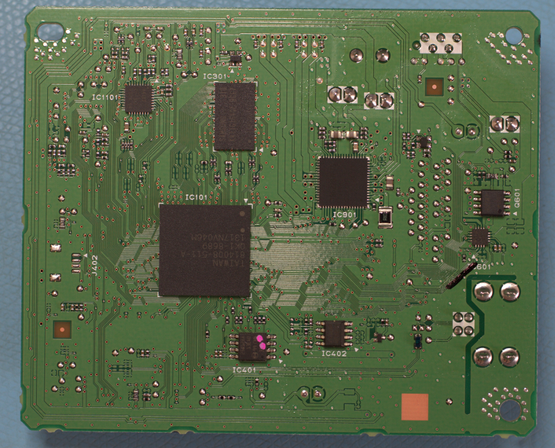
The big square chip is the ASIC. The rectangular chip above is RAM (for document and working memory). The chip with the pink dots is a 16MB serial Flash RAM (there is another 4MB Flash chip on the other side), and the small chip to its right is a serial EEPROM chip. The Flash RAM chips are used for storing firmware, and the EEPROM for storing configuration settings. The Flash and EEPROM chips are readily identifiable from their markings, and datasheets are freely available.
This board from an old Brother printer has (from left to right) two ROMs, three RAM chips and an ASIC:
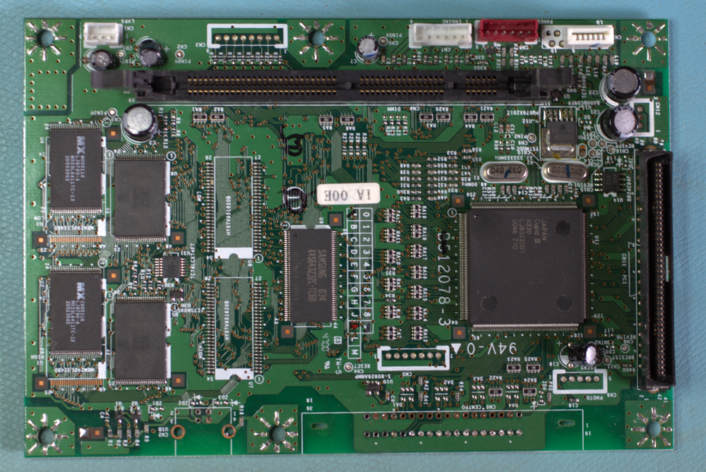
Once again, the ROM chips have readily obtainable datasheets.
Data analysis
Once you’ve got the data on your computer, the first thing to do is to convert it back to binary (most likely you wrote it down the serial connection as ASCII/hex data – well, that’s what I do). Now, I do all my analysis using Linux, so if you’re using Windows or a Mac, you’ll need to work out what the equivalent commands are…
Once you’ve got a binary blob that contains the data you extracted from the target, you’re ready to start doing some investigation. The first sanity check is that the size of the data file should match the capacity of the target chip, so you know you haven’t lost or corrupted your data.
Next, and I think the most exciting part, is to look at the string data by running “strings” or “hexdump” over the binary data and extract out the readable text. If you start to see human-readable text or data, then you know that you’re on the right track. There is going to be all kinds of useful information right there. Who knows, if you’re lucky you might find things like passwords, debug commands, public keys, URLs etc. Even if you don’t find stuff like that, the text you do find will help guide your further explorations. In one data dump I looked at, most of the data seemed to be random, but there were some error messages that suggested that some decompression code was being used. A quick Google revealed that the dump contained code from the “zlib” library, and that I needed to look for “deflated” data regions and decompress them (I was looking at a firmware blob, where most of the content was compressed). As you can imagine, this is where a bit of practice and intuition will serve you well. Plus, you can always Google for more information.
If you’re looking at executable code, the most likely layout is going to be repeated sections of code and data (including strings). One of the skills of reverse engineering is working out which parts are the executable code, and what kind of instructions they contain. There are some clues you can use to help guess what processor is being used. For example, if nearly every 4th byte is of the form E* (in hex), you can be confident that you are looking at ARM instructions. One trick I have used is to Google sequences of 4 or 8 hex bytes (which may be 2-4 instructions); often you’ll get a match which tells you the processor. There’s also a very handy site, called The Online Disassembler, which lets you paste some hex data and try disassembling it using different processors. Once you’ve worked out what processor you have, it’s time to start working out where the functions lie. “Call” and “return” instructions are very useful for this. Some higher priority things to look out for are boot/startup code (often near the start of the blob) and some clues about the device memory map (where is ROM, RAM, memory-mapped hardware located?).
At the end of the day, it’s going to take some effort to start working out what the code does. There are some tools that can make things easier for you, for example IDA ($$) or radare (free). Or maybe you could get a gcc-based cross-compiler with disassembler (objdump) and write some scripts to manage things.
Reverse engineering example
I pulled a board out of an old Brother HL-1435 printer that was no longer useful. It was fairly simple, with a pair of 2MB DRAM devices (not much memory for a printer these days), a large ASIC containing a processor and other logic. The main chip of interest is a Macronix MX23L8111 1MB Mask ROM, whose datasheet is available on the Internet. The exercise here was to extract the software from the ROM.
Extracting the software
I wired up the ROM to a home-made header so that I could attach it to a prototyping breadboard. Now, this chip has parallel addressing, so that means I need to connect to 20 address lines and 8 data lines, along with 4 other control lines. To achieve this, I need a reasonably studly microcontroller with lots of I/O ports. My usual go-to for this kind of thing is an ATMEGA644, but here it doesn’t quite have enough I/O capacity (I need to use 4 lines for JTAG programming and another for the serial output). So, I went up to an ATXMEGA16A4.
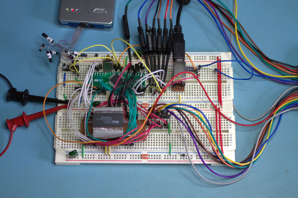
Here’s what the setup looked like. It’s not as complicated as it looks! The microcontroller is on the green carrier board at the top left, which the ROM below it. There are a bunch of wires connecting them together. The silver rectangular device to the right is a handy serial-to-USB gateway that lets me connect serially to a USB port on my desktop. The JTAGICE3 programmer is the silver box at the top, 3.3V power comes in from the left and the coloured wires disappearing off to the right go to a Saleae Logic 16 Logic Analyser.
At the same time as I am putting this together, I whipped up a simple C program to load onto the microcontroller.The program cycles through the ROM’s address space and reads back the byte of data at each position. The data is converted to a hex string and written down a 115200 baud serial connection to my computer.
Once I’ve double-checked all the connections I can power it up and load the software onto the microcontroller. After some debugging, I can see plausible-looking hex data being printed on a terminal program running on the computer. I replaced the terminal program with a simple perl script that reads data from the serial USB port and saved it in a file, and reset the microcontroller so that it restarts at address zero. After about 1/2 hour it is done and I can shut everything down.
The final step is to convert the hex data back to binary using another perl script, and start looking at the data. The first step is to run “strings” over the data. When I see text like “AM TEST DRAM OK” and “Drum Life”, I can be pretty sure I’ve managed to get the data out intact!
You can see the software I used here:
https://github.com/rolfeb/proj-romdump-MX23L8111
Decoding the data
[To be continued]
Thank you for this. This is pure gold.