How magnetic core memory works
Looking back at computing history in interesting. Firstly, the concepts and hardware implementations are usually simpler and easier to understand – I bought my first computer in the early 1980s and I pretty much understood the whole thing down to the IC level. That doesn’t really work today… Secondly, people made do with much less capability, and yet still got a lot of serious work done. We are pretty spoiled today.
Anyway, one day I noticed that you can actually buy ferrite cores of the type that were used in core memory boards on eBay, so I started wondering whether it was possible to create my own memory using this.
But first, I had to learn a bit about magnetic core memory.
History and context
Before core memory, storage options were pretty primitive. People were using things like Williams Tubes, delay lines and drum memory. These were either painfully slow, low in capacity, or both. And they were expensive.
Core memory came along at a time when the use of computers exploded from research to large-scale commercial use. It could be deployed on standard boards that could be installed in computers, was significantly faster and could be scaled up to much larger capacities.. During the life span of core memory, costs dropped to something like 1 cent per bit. Boards providing 32 kB of memory were not uncommon.
The heyday of core memory was around 1960 to the late 1970s. Eventually, semiconductor memory became cheap enough to supplant it, and of course we know today how that has grown.
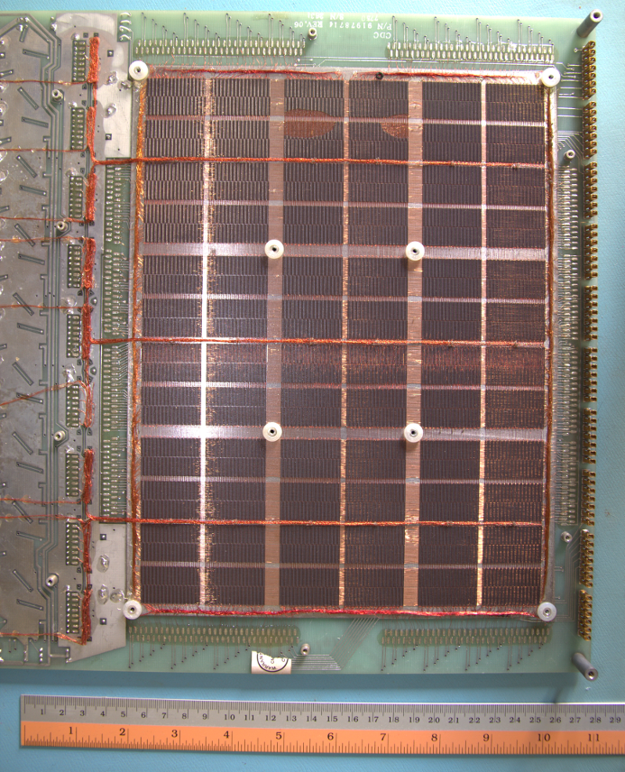
I have a surplus core memory board that provided 16k words (16-bit) of memory, which I bought off eBay a few years ago. It was manufactured by General Automation Inc, probably in 1977. It comprises 2 boards stacked together. The first contains all the interface logic and drivers, and the second contains the magnetic cores. The cores are small. Really small.
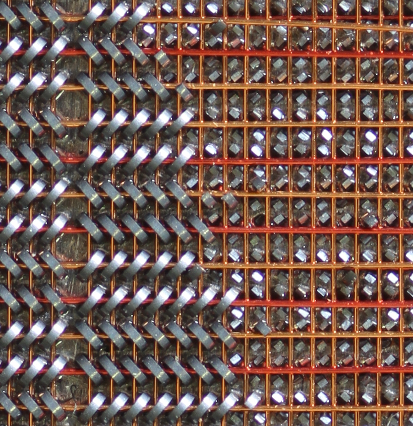
Here is the core memory with the interface board removed. There were 294,912 individual cores on this board (note that there are 9 major blocks, which means this board supported a parity bit). Each of the smallest blocks contained 4096 bits of memory.
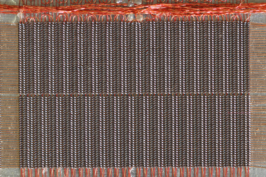
Here is a close-up of one of the 4kb blocks:
How core memory works
The operation of core memory is actually pretty simple – all you need to know is a little bit of high-school physics.
First of all, you need to know that moving charges (I) create a magnetic field (B) in the direction according to the right-hand rule:
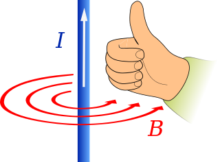
In our situation, the moving charges are electrons in a wire (a current). The magnetic field wraps around the wire. If we place a ring of magnetic material around the wire, then the current flow can create a permanent magnetic field in the ring. The direction of the magnetic field depends on the current direction – reverse the current and you reverse the direction of the magnetic field. This suggests that maybe we can use the direction of the magnetic field to represent a binary digit…
To get from this basic physical effect to a storage mechanism, we need two more insights.
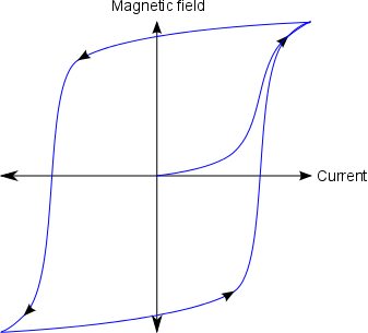
Firstly, An Wang created a way to store and retrieve data from a magnetic ring. He used ferrite, which has a key property, that the strength of the magnetic field induced by a current is not linear. Instead, the material resists the creation of the magnetic field until the current reaches a threshold value. After this point, a small increase in current results in the creation of the full magnetic field. Similarly, if the current is reversed, the magnetic field resists change until the reverse current reaches the threshold, after which the magnetic field “flips” over to the other orientation. This is a classic hysteresis response, and is shown in the following diagram:
Now… here is the second bit of physics you need to know: a changing magnetic field can induce a current in a nearby conductor (this is how a generator works). So, if we put a second wire through the ring, the flipping of the magnetic field will create a current in the wire, which we can detect as a small pulse. So now, we have what we need to store a bit in a ferrite ring:
- Choose one current direction as representing 0, and the other as 1.
- Write the desired bit value by sending some current down the write wire in the appropriate direction.
- To read the value, just write a zero value and look for a pulse in the sense wire. If was see one, we know the previous value was one so we need to rewrite the value back to one. If there was no pulse, then the previous value was already zero and we don’t need to do anything more.
This invention was patented US 2,708,722.
By itself, this scheme is not very efficient. Each bit needs a set of bidirectional drivers at each end of the write wire to drive the current in either direction. This doesn’t scale up from a hardware cost perspective.
Enter Jay Forrester, who realised that you don’t need to supply the threshold current through just one wire. Instead, you can send half the necessary current through two wires in the same core. He proposed arranging ferrite cores in a rectangular matrix, with each core encircling one vertical and one horizontal drive wire. Each of the wires can be driven by just over half the threshold current. So, if one vertical wire and one horizontal wire is energised, the only core that will see the threshold current is the one at the intersection of the two wires.
This is a much more efficient scheme. It was patented as US 2,736,880.
So, now we have a rectangular array of cores, each of which has two drive wires that are addressed in (x, y) coordinates with the current direction determining the value written. The cores also have a sense wire for reading the pulse. However, you only need one sense wire for whole matrix as you are only writing a single core at a time (you only need to know that one of the cores flipped or not).
Many core memory arrays also have a 4th wire, known as the inhibit wire. Like the sense wire, one inhibit wire runs through all the cores. The purpose of the inhibit wire is to optionally provide current in the opposite direction to the write current, through the core being written. This will cancel out some of the magnetic field, and prevent the core from changing. Why would you want to do that? The answer is that it lets you easily stack multiple planes of core memory, all sharing the same drive wires. Without the inhibit wire, this would cause the corresponding core in each plane to be written. By sending the appropriate current down all the inhibit wires except one, we can ensure the write only affects the desired plane. The inhibit wires is an efficient way to scale up a system by adding multiple memory core planes. The alternative would be to make the matrices bigger and bigger, but eventually current losses and crosstalk make this impractical.
So, that’s really you really need to know.
The hard part is manufacturing, especially with the usual demands for increasing capacity (making everything smaller) and performance. At their peak, memory boards could provide tens of kilobytes with an access time down to 1μs (corresponding to a clock rate of 1MHz). And of course, core memory has one huge advantage that I haven’t mentioned yet – it retains its contents when the power is turned off!
Core memory assembly required some pretty special techniques. Originally they were assembled by hand, but eventually various jigs and so forth were created to make things easier. IBM described some of how this was done in their 1969 paper, “Ferrite Core Planes and Arrays: IBM’s Manufacturing Evolution” [PDF].
My memory board has some damaged areas, which reveals that the bottom of the cores are embedded in some resin. So the cores were probably assembled into a positioning jig (probably using a vacuum/shaker table) and then glued onto the board. Once the glue dried, the cores were all nicely aligned to allow the wires to be fed through. You can see this damaged area here:
Building a board
So, now I thought that I’d like to try to reproduce a memory board. I order some ferrite cores from eBay, and a few weeks later they arrive from a gentleman in Bulgaria:
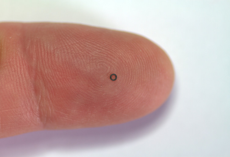
Wow, they’re smaller than I expected! I had some 0.2mm enamelled wire, which should be fine enough to be able to thread 3 wires through the core…
Now a number of other people have put up resources detailing how they created some core memory, and I borrowed heavily from them (see the links at the bottom).
My first step was to verify my understanding of how reading and writing worked, so I mounted a single core on a piece of perfboard and made up a breadboard test circuit with a microcontroller to drive it. The easiest test was to write 0, 0, 1, 1, and to check that I could detect a pulse only when the stored value was changed. After some tweaking of current values, I was able to verify that the proof of concept worked. Here’s a screen grab from my oscilloscope:

The yellow line is the signal on the sense wire. There are 3 spikes from write operations (a negative one on the left, and positive ones in the middle and on the right). The small dip just to the right of the middle is the signal from the reversing of the magnetic field in the core, about 50mV delayed about 800ns from the pulse. Success!
I spent some time creating a circuit for an 8×8 matrix, and then I designed a PCB for it. I sent the design off to Osh Park for fabrication and when it came back , I spent some time threading wires through tiny cores (3 wires in each one!) and then put the rest of the components on board. Here is what it looks like:
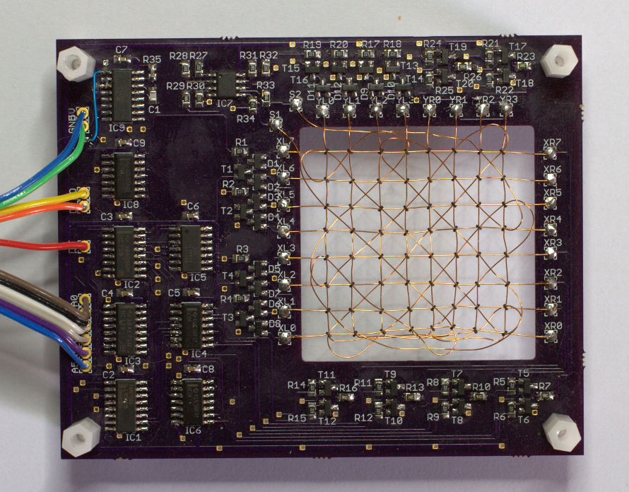
The ICs on the left decode the address and work out which horizontal and vertical wires to write to, and which direction the current should flow. Around the matrix are transistors making up H-bridge circuits to control the write signals. The small IC near the top detects the small signals from the sense wire.
I was a bit concerned about wiring up the cores, but it turned out only taking a few hours. The second of the vertical/horizontal wires turned out to be the hardest, because you are pushing wire through cores at 45° orientation. The sense wire was last, but this was much easier than I expected because it passes through the cores along their axis.
There was only one wiring error (bodge wire, top left corner) but that was easy to detect and fix. The next step was to connect it up to a microcontroller that was tasked with writing values to the core and reading them back. The results were sent down to my computer over a serial line. Success! I was able to verify that it was working by waving a magnet near the cores and seeing the values get corrupted… 🙂
Conclusion
As with all projects like this, getting it working was really most of the fun. It was great to be able to understand the physics of how core memories work and to be able to replicate it on my workbench.
Of course, hooking the thing up to a microcontroller on a breadboard isn’t terribly satisfying. Somewhere at the back of my mind is the idea that maybe version 2 could have a USB interface, so you could just connect it to any computer…
Links to similar projects
I haven’t done anything new in my project. Here are some links to people whose pages inspired me to do this.
- “Coincident Current Ferrite Core Memories” (James R. Jones details a project to add 4K core to his computer, from Byte magazine July 1976)
- “Magnetic Core Memory Logic Details” (James R. Jones’ website with more information on his core memory board)
- “Magnetic core memory reborn” (Ben North and Oliver Nash present their design for an Arduino core memory board)
- “Magnetic Core Memory Systems” (Brent Hilpert discusses some interesting implementation details used in core memory boards)
- “Memory Drivers and Sense Amplifiers” [PDF] (TI design note from 1973 explaining how to use their standard ICs to interface to core memory)
Great article woulb be nice to try it my self.
I really really really appreciate this article!
Thank you!
Hello, thank you for this wonderful article. I was just wondering if you (or anyone else) has any information on the material used for these ferrites. It’s important that the ferrite cores have the correct hysteresis curve and this is where my research has proved unsuccessful. Actually, some articles say this will work with almost any ferrite so I am hoping to make a test setup so I can test different cores to see what works.
I will probably post back the results here. However, If anyone would answer my question it would be much appreciated.
The cores look like they were manufactured some time ago, in East Germany by the VEB Keramische Werke, Hermsdorf. When I bought them on eBay they had were described as “New Old Stock, Military Surplus”; they had a part number “5221.3-2113.35”. If you search on eBay (or Google) for that part number you’ll see that they are still being sold.
I expect that they were made specifically for use in core memory, and so should have the right composition. When I searched on the Internet for VEB Keramische Werke, I even found some old catalogues, but I couldn’t see any listing for ferrite cores of that size…
Great project and write up! Did you know that “Magnetic core memory reborn” (Ben North and Oliver Nash) inspired an Arduino shield? It’s here on Tindie: https://www.tindie.com/products/kilpelaj/core-memory-shield-for-arduino/
And that inspired me to do some experiments to make the cores interactive and visual. You can see that project taking shape here: https://www.element14.com/community/community/project14/electromagnetism/blog/2019/02/22/flipping-core-memory-bits-directly-with-a-magnetic-stylus
Any chance you are selling your 8×8 core configurations?
Hi Rolfe. Great project! Do you have any spare boards, blank or otherwise, left over? I’d be interested in one, because I’d like to expand my project from 4×8 to 8×8. If you’d like to see what I’m working on, you can check it out here: https://hackaday.io/project/163976-interactive-core-memory-shield-using-led-matrix
Hi, a nice work, thanks for the report about. The supplier from Bulgaria offer those ferrites as so, but offer ferrites ‘Miniature RAW FERRITE Magnetic CORES 5221.3-3114.53’ too. They looks really small on the photo on ebay, little smaller than core you used. The oscillogram in your article shows memory read time about 800 ns at minimum. It looks too slow for my TTL computer (currently with MOS memories), I need below 600 ns for read the cell (in the case the partially erased information will be magnetised back instantly in next 600 ns) and below 1200 ns for rewrite the cell (unfortunately in the case, that each of four bits of the word will be set or reset on separated accesses simultaneously, i.e. each bit with own coordinate independent decoder etc.). The article ‘Coincident Current
Ferrite Core Memories’ seems more optimistic with a 400 ns peak of the read pulse with cores available in 1976. There are two hopes: the core 5221.3-3114.53 (or other available) is smaller and faster, maybe newer and better, and/or perhaps is possible to use a bit stronger currents in coordinate lines than you’ve used. Do you have any opinion about those possibilites, please? Did you really used the bigger of both cores from Bulgaria, did you use a suittable currents for core coordinates, both about 0.7 of the current, what the core need to switch the flux? Next idea, to use the wire for an oposite magnetisation of all cores (similar to ‘inhibit’ wire, but in 2D grid) to increase the coordinate currents, seems not to be very practical.
Thats the way great engineers work 🙂
“I was able to verify that it was working by waving a magnet near the cores and seeing the values get corrupted… 🙂”
Amazing article, thank you very much for helping to understand why the inhibit wire is needed, this is the best article about Core Memory that I red.
[…] Bozier, R. (2015, August 10). How magnetic core memory works. Retrieved February 16, 2021, from https://rolfebozier.com/archives/113 […]
Rolfe, your project has been an inspiration in my journey to create an interactive core memory kit for like-minded people who want to experiment with Core Memory. I think you will appreciate seeing this version of Interactive Core Memory in action at https://www.Core64.io/
Hi Andy,
That is absolutely awesome!